

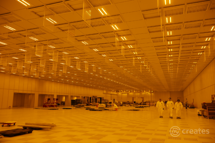
Governor Kathy Hochul right this moment introduced the start of set up of Tokyo Electron’s modern 300 mm wafer coater/developer system designed to help the following era of semiconductor manufacturing at NY Creates’ Albany NanoTech Complicated. This software, referred to as the CLEAN TRACK™ LITHIUS Professional DICE™, applies and processes a light-sensitive layer on silicon wafers, which is the platform upon which pc chips are constructed. This permits researchers to manufacture the minute patterns wanted for the following era of superior processors, reminiscence, sensors and extra. That is the primary main piece of kit to be delivered for the forthcoming Excessive NA Excessive Ultraviolet (EUV) Lithography Middle at Albany NanoTech, which will probably be North America’s first and solely publicly owned, accessible Excessive NA EUV Lithography analysis web site.
“New York State is main the nation in semiconductor manufacturing and R&D, and the set up of this software for the Excessive NA EUV Lithography Middle will enable New York to stay on the forefront of chip innovation,” Governor Hochul stated. “This announcement showcases the significance of public-private partnerships and the way we are able to work collectively to ship for New Yorkers and the nation, offering cutting-edge expertise to help groundbreaking manufacturing proper right here on this state.”
Within the coming months, ASML’s Excessive NA EUV lithography system, arguably essentially the most superior machine ever created, will arrive in sections and be put in inside the brand new NanoFab Reflection (NFR) constructing. “First gentle,” when the software’s EUV gentle is first turned on, is anticipated earlier than the tip of the yr. This progress follows NFR’s “topping-out” milestone, attended by Governor Hochul in December, when building groups put in place the constructing’s ultimate metal beam.
Governor Hochul introduced Creates’ Excessive NA EUV Lithography Middle in December 2023, a $10 billion partnership which incorporates $9 billion in business funding and $1 billion from Empire State Improvement, with leaders from the semiconductor business similar to IBM, Micron, Utilized Supplies, Tokyo Electron, and others. The initiative is establishing a next-generation semiconductor analysis and improvement middle at Creates’ Albany NanoTech Complicated to help the R&D of the world’s most advanced and highly effective semiconductors.
Empire State Improvement President, CEO and Commissioner Hope Knight stated, “New York State has firmly established itself as a worldwide hub of cutting-edge semiconductor analysis, anchored by world-class belongings just like the Albany NanoTech Complicated and strengthened by unprecedented public-private partnerships. By way of focused, strategic investments, we’re constructing a sturdy ecosystem that accelerates innovation, helps next-generation applied sciences, and attracts business leaders. These efforts are usually not solely advancing the way forward for chip R&D, but additionally creating high-quality jobs, increasing alternative, and securing New York’s management on this important business for many years to return.”
Senator Charles Schumer stated, “Essentially the most cutting-edge excessive ultraviolet chip-making expertise on the planet is being put in proper now within the Capital Area’s yard. It is a main leap ahead that can propel American discoveries in chipmaking that scientists right this moment can’t even fathom. My CHIPS & Science Legislation has delivered main federal funding throughout Upstate NY to assist communities from Syracuse to Albany paved the way in semiconductor manufacturing, and this state-of-the-art Excessive NA EUV Lithography Middle will assist supercharge these efforts. With this new superior chipmaking software being put in, Albany NanoTech is main the nation in guaranteeing America stays forward of China within the race to construct the way forward for expertise. I’m grateful for Governor Hochul’s partnership in guaranteeing the following era of microchips will probably be developed right here in America, in Upstate NY, not abroad.”
NY Creates President and CEO Dave Anderson stated, “As we start putting in the primary main software for our Excessive NA EUV Lithography Middle, we’re taking an vital step towards enabling essentially the most superior semiconductor analysis capabilities on the planet. Tokyo Electron’s LITHIUS Professional DICE system will play a foundational function in supporting Excessive NA EUV operations and accelerating breakthroughs with our business companions, and we’re thrilled to be coordinating this preliminary effort with our longtime collaborators TEL Expertise Middle, America, based mostly at our web site, in addition to ASML. This progress displays New York’s strategic investments and our group’s dedication to driving the following era of semiconductor innovation for the U.S. proper right here at our Albany NanoTech Complicated.”
TEL Expertise Middle America (TTCA) President Alex Oscilowski stated, “The set up of the LITHIUS Professional DICE system on the Albany NanoTech Complicated Excessive NA EUV Lithography Middle underscores what is feasible when the semiconductor ecosystem comes along with a shared dedication to innovation. As Excessive NA EUV comes on-line, it can speed up advances in AI, high-performance computing, and the applied sciences that can form how the world connects, computes, and creates.”
ASML Enterprise Line Excessive NA EUV Head Peter Vanoppen stated, “Excessive NA EUV is a important enabler of the following era of semiconductor innovation, and the brand new Excessive NA EUV Middle on the Albany NanoTech Complicated will create a useful R&D atmosphere for business and analysis companions to collaborate on essentially the most superior lithography expertise. ASML is proud to help next-generation improvement on the Middle with the forthcoming supply of an EXE:5200B lithography system, which is able to assist strengthen the U.S. semiconductor ecosystem and speed up innovation for the long run.”
Micron Expertise, Inc. EVP and Chief Expertise and Product Officer Scott DeBoer stated, “The arrival of the primary Excessive NA EUV course of software at NY Creates marks a significant milestone for superior semiconductor R&D in New York and the U.S. The Excessive NA EUV Lithography Middle is important for constructing the R&D ecosystem that drives next-generation Reminiscence and Logic applied sciences, enabling future high-performance computing and superior AI. This enhances Micron’s mega fab funding, which is able to create 50,000 jobs by supporting the analysis, expertise and innovation pipeline wanted for long-term success. Micron is proud to collaborate at Albany NanoTech, serving to strengthen American management and resilience in semiconductor manufacturing.”
IBM Analysis GM of IBM Semiconductors and VP of Hybrid Cloud Mukesh Khare stated, “This milestone is a crucial step ahead for the Excessive NA EUV Lithography Middle and the innovation ecosystem on the Albany NanoTech Complicated. IBM has a protracted historical past of pioneering advances in chip expertise, together with the world’s first 2 nm node chip, unveiled in 2021. Excessive NA EUV is important for sub-2 nm scaling, and this functionality will speed up breakthroughs that can form the way forward for computing.”
NY Creates’ Excessive NA EUV Lithography Middle already gives business accessibility to plain NA EUV Lithography capabilities. Excessive NA EUV lithography capabilities will enable chip improvement on the most superior expertise nodes whereas serving as a platform for added associate progress with entry to Creates’ cutting-edge R&D infrastructure.