

Electroninks is a kind of firms that might change the way in which manufacturing works. The Texas-based agency makes conductive inks, and in copper, nickel, gold, platinum, and silver, these inks may be 90% conductive whereas additionally being safer and manufacturable at scale. We beforehand talked to their CEO Brett Walker on the 3DPOD, and the corporate’s journey, from taking cash from In-Q-Tel to working with FujiFilm, Scrona, and Sakata, has been going from power to power.
Now, the College of Texas at Austin (UT Austin) has chosen Electroninks to be a key supplies provider for its work underneath the Protection Superior Analysis Tasks Company (DARPA) Additive Manufacturing of MicrosystEms (AMME) program. AMME‘s “final purpose is to reveal a novel, practical microsystem that integrates a number of supplies inside a single construction, enabling designs unattainable with typical strategies.” They wish to create new supplies to make use of for 3D printing microelectromechanical methods, or MEMS—sensors coupled with mechanical parts and electronics, all made on-demand in novel, conformal, or different shapes. Primarily, they’d prefer to print an inertia sensor, or possibly even a listening to assist. However, in fact, they’ll already do that, so I believe AMME is, in true DARPA fashion, aiming a bit larger, and so they truly wish to print your cellphone. I’m watching AMME like a hawk, and am tremendous enthusiastic about this program that needs to commercialize some really astounding expertise. After a dozen Israeli startups made it to market, the US needs to strive, too.

Electroninks says that,
“AMME seeks to remodel microsystem manufacturing by pioneering developments in high-speed, high-volume, and high-resolution multi-material manufacturing. This cutting-edge additive manufacturing course of will improve industrial units with next-generation built-in applied sciences whereas enabling speedy adaptability to evolving mission necessities—very like additive manufacturing has revolutionized complicated prototyping. By way of AMME, DARPA goals to interrupt by means of the inherent limitations of conventional microsystem fabrication, unlocking new prospects for innovation and scalability.”
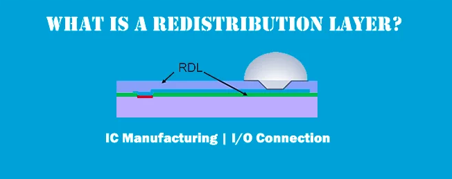
The corporate will work with conductors and insulators throughout the identical part utilizing 3D interconnects and RDL, a redistribution layer in IC Packaging; it is a key strategy to join the chip to the surface world. With 3D interconnection, a number of chips are positioned on a wafer in a stack, saving house and rising performance. These are applied sciences which are very related for essentially the most superior units that you just use on daily basis. The corporate says that, “by creating revolutionary conductive supplies optimized for high-speed, large-area lithographic patterning, Electroninks’ contributions will assist overcome basic limitations in present semiconductor packaging processes.”
One other approach that AMME might be related is that it’s tremendous manufacturing-focused and meant to commercialize this expertise, not simply be an idea automobile. The corporate can be specializing in scalability and high-volume manufacturing, and hopes that this may result in iterative manufacturing of electronics. Moreover, IC packaging may turn out to be extra environment friendly and doubtlessly cut back vitality consumption.
Picture: Nicely Executed Know-how
As a part of the AMME program, UT Austin’s Division of Mechanical Engineering is working with a number of business leaders and educational establishments on improvements in semiconductor packaging. Electroninks will provide the mandatory supplies for AMME’s new 3D interconnection methods. UT Austin’s Professor Michael Cullinan acknowledged,
“AMME represents a big step ahead in semiconductor expertise, addressing important challenges in AI {hardware} and superior packaging. By integrating cutting-edge supplies with state-of-the-art holographic lithography, we goal to drive new ranges of effectivity and functionality in semiconductor manufacturing.”
Electroninks CEO Brett Walker stated,
“We’re clearly poised to be a big accomplice for this consortium and play a key function in fulfilling DARPA’s targets. That is nice information for the State of Texas, innovation and the way forward for expertise.”
AMME may finally change what number of issues are made. There are lots of people worldwide working in IC packaging, photonics, and plenty of associated fields. However, by extra effectively connecting and constructing electronics, AMME may redefine how MEMS and different packages work, and the way properly they work. Packages might be optimized in a very new strategy to be unfold out, made conformal, or compacted to suit inside units like your cellphone. This can be a nice win for Electroninks and will result in a breakthrough in IC packaging and past within the years to come back.
Subscribe to Our Electronic mail E-newsletter
Keep up-to-date on all the most recent information from the 3D printing business and obtain data and presents from third occasion distributors.
Add your 3D Fashions and get them printed rapidly and effectively.

